User guide
This guide walks through using padne to analyse the power delivery network of a KiCad project — from describing the lumped circuit attached to the board, through running the solver, to inspecting the result.
How padne works
padne is a KiCad-native power delivery network analysis tool. It uses the finite element method to simulate the DC voltage drop on printed circuit boards, which lets you identify resistive bottlenecks, design high-current distribution networks, or even shape complex heating elements.
The PCB copper itself is meshed and solved as a 2.5D conductor stack; the rest of the circuit — sources, sinks, dependent supplies — is described as a small lumped network attached to the mesh via text directives placed in your KiCad schematic. A typical schematic might look like this:
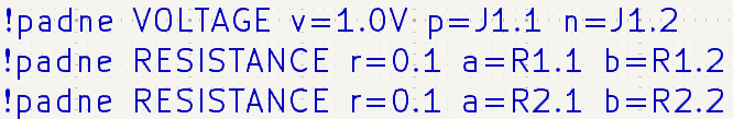
Every directive starts with !padne followed by the directive name
and its parameters. The complete syntax is documented in the
Directive reference.
Running the solver
To run the solver and display the solution in one step:
padne gui my_project.kicad_pro
You can also save a solution and display it later:
padne solve my_project.kicad_pro pdn.padne
padne show pdn.padne
For advanced visualization, export the solution to ParaView/VTK:
padne paraview pdn.padne output_directory/
This creates a separate .vtu file per layer that can be opened in
ParaView for further visualization and analysis.
Tip
Run padne gui --help to see the exposed mesher parameters.