Test board
In addition to many virtual test cases, the padne test suite also contains a design for a physical test board. This board contains various “test cases” that are designed as a stress test and reference for padne to guide further development.
Board design
At the moment, a single test set is implemented in the test suite: test_set_1. This board contains a calibration ladder, various via configurations, some geometry stress tests and several resistor chains with various pad connections.
Usage guide
The board is designed to be used in a standard four-point measurement way. Two convenience connectors wired in series are available to connect a current source and a current meter.
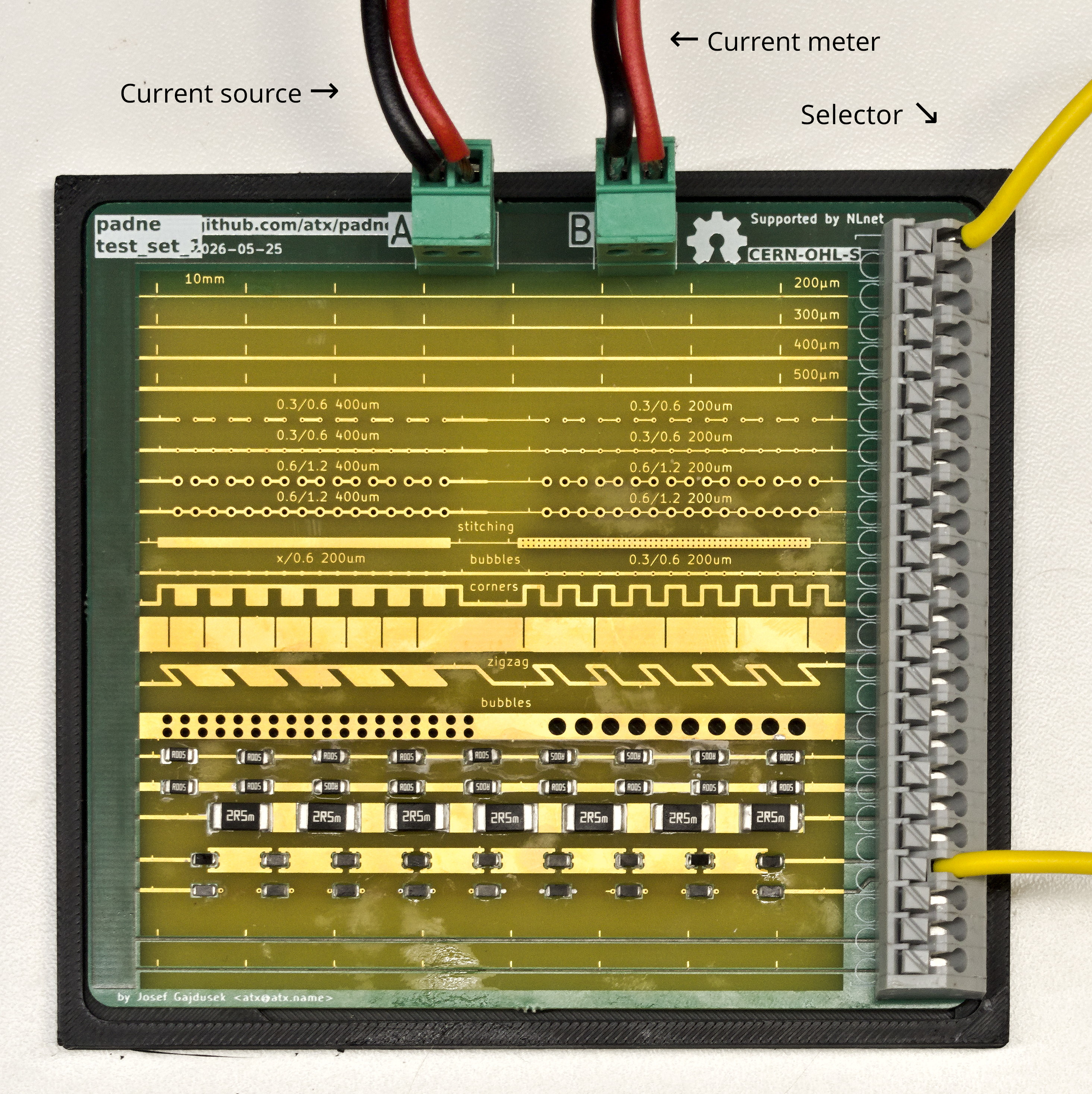
Start by connecting the current source to the connector labeled A and the current meter to the connector labeled B. The large terminal block on the right hand side is used to select a test case to be measured by connecting the topmost pin to the corresponding test case pin.
Calibration ladder
The first step is measuring the calibration ladder. Each trace of the 0.2 mm / 0.3 mm / 0.4 mm / 0.5 mm ladder is measured at the farthest tick mark of the trace. Enter each measurement into the corresponding place in the test case definition.
Then, the calibration fit can be observed by executing:
python3 tests/test_sets.py calibrate test_set_1_aisler
The calibration fit is a two parameter regression that produces sheet conductance and overetch. The overetch is an offset of the inferred trace width from nominal (the etching process is assumed to consume a constant amount of material from each side of a trace).
The sheet conductance is the directly measured quantity. The thickness is inferred from it under an assumed bulk copper resistivity, so it is only indicative. Plated outer-layer copper tends to run more resistive than bulk, which would put the true thickness above the figure shown.
The results are printed to the console and for the test_set_1_aisler
look like this:
sheet conductance : 2559.8 S
thickness vs ref  : +22.9% (implied 43.02 um, ref 35.0 um)
overetch delta    : 70.49 um

rung            w_nom/mm    R_meas/ohm     resid/ohm
TP61-TP60          0.200          0.21      -0.00114
TP63-TP62          0.300          0.12      0.000853
TP65-TP64          0.400        0.0827     -0.000289
TP67-TP66          0.500        0.0637       3.3e-05
Note
Note the particularly high overetch for the Aisler produced test board. It is to be determined whether this replicates across multiple manufacturers. The narrowest rung is 0.2 mm, well above the overetch, so the figure is somewhat extrapolated. Also note that overetch compensation is currently not supported by padne and is to be implemented in the future.
The test suite itself
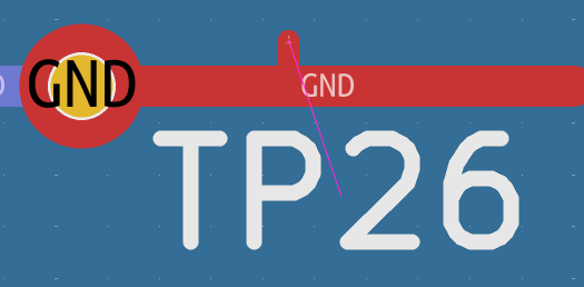
The individual measurements are defined as a list of voltages measured between test points given by their designator. In the PCB design, the test points are implemented as small pads placed within the design. Usually, a small “tick” mark is placed on the trace to make visual registering of the test point easier.
The measurement pairs are defined in the test_sets.py file of the test suite. Although in theory each individual test case can have its own injected current value, the nominal current is currently defined to be 1 A for all of the test cases.
A test report can then be generated by executing:
python3 tests/test_sets.py report test_set_1_aisler
Note
The test suite automatically corrects for the sheet conductance from the previous step but does not (yet) correct for overetch. Since resistance scales as 1/w, this exposes a systematic underprediction on narrow traces on the Aisler-produced board: about 35% on the 0.2 mm rung, falling to 14% at 0.5 mm.
Notes on the test board
As of now, test_set_1 has been manufactured by Aisler
and the results are available in the test_sets.py file of the test suite.
The measurements committed to the test suite have been done with this equipment:
Miniware MDP-P906 programmable power supply
UNI-T UT61E digital multimeter used as the current meter
EEVBlog 121GW multimeter as the voltage meter